| CPC H01L 27/124 (2013.01) [G02F 1/1333 (2013.01); G02F 1/1343 (2013.01); G02F 1/136213 (2013.01); H01L 27/1225 (2013.01); H01L 27/1259 (2013.01); H01L 29/24 (2013.01); H01L 29/7869 (2013.01); H01L 29/78618 (2013.01); H01L 29/78696 (2013.01); G02F 1/136227 (2013.01); G02F 1/136231 (2021.01); G02F 2201/50 (2013.01)] | 15 Claims |
|
1. A display device comprising:
a pixel portion comprising:
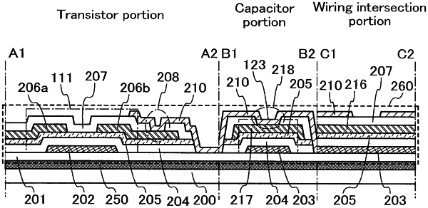
a first conductive layer comprising a region in contact with an insulating surface;
a first insulating layer comprising a region in contact with an upper surface of the first conductive layer;
a first oxide semiconductor layer comprising a region in contact with an upper surface of the first insulating layer, the first oxide semiconductor layer comprising a channel formation region of a transistor;
a second conductive layer comprising a region in contact with an upper surface of the first oxide semiconductor layer;
a second insulating layer over the first oxide semiconductor layer and the second conductive layer; and
a third conductive layer electrically connected to the second conductive layer, the third conductive layer comprising a region over the second insulating layer; and
a connecting portion comprising:
a fourth conductive layer comprising a region in contact with the insulating surface, the fourth conductive layer comprising the same material as the first conductive layer;
the first insulating layer comprising a region in contact with an upper surface of the fourth conductive layer;
a second oxide semiconductor layer comprising a region in contact with the upper surface of the first insulating layer; and
a fifth conductive layer over the second oxide semiconductor layer, the fifth conductive layer comprising the same material as the third conductive layer,
wherein the first conductive layer is configured to serve as a gate electrode of the transistor,
wherein the second conductive layer is configured to serve as one of a source electrode and a drain electrode of the transistor,
wherein each of the first conductive layer and the fourth conductive layer comprises a stacked structure comprising a titanium layer and a copper layer over the titanium layer,
wherein the first insulating layer and the second oxide semiconductor layer comprise a contact hole, and
wherein the fifth conductive layer is electrically connected to the fourth conductive layer through the contact hole.
|