| CPC H01L 27/1229 (2013.01) [H01L 21/02565 (2013.01); H01L 21/02672 (2013.01); H01L 27/1225 (2013.01); H01L 27/14632 (2013.01); H01L 27/14687 (2013.01); H01L 29/04 (2013.01); H01L 29/0847 (2013.01); H01L 29/24 (2013.01); H01L 29/41733 (2013.01); H01L 29/66742 (2013.01); H01L 29/66969 (2013.01); H01L 29/7869 (2013.01); H01L 29/78693 (2013.01); H01L 27/1156 (2013.01)] | 10 Claims |
|
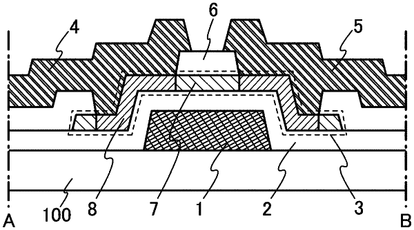
1. A light-emitting device comprising a pixel, the pixel comprising:
a transistor comprising:
a first conductive layer;
a first oxide semiconductor layer comprising a channel formation region of the transistor;
a second conductive layer in contact with the first oxide semiconductor layer; and
a third conductive layer in contact with the first oxide semiconductor layer;
a capacitor comprising:
a fourth conductive layer; and
a second oxide semiconductor layer over the fourth conductive layer;
a first insulating layer over the second oxide semiconductor layer;
a fifth conductive layer over the first insulating layer, the fifth conductive layer being electrically connected to the second oxide semiconductor layer;
a second insulating layer over the fifth conductive layer;
a third insulating layer over the second insulating layer;
a light-emitting element comprising a pixel electrode; and
a color filter layer between the second insulating layer and the third insulating layer,
wherein a width of the second oxide semiconductor layer is larger than a width of the fifth conductive layer in a cross-sectional view of the light-emitting device,
wherein the pixel electrode is electrically connected to the second conductive layer through a first opening in the third insulating layer and a second opening in the second insulating layer,
wherein the color filter layer does not overlap with the first conductive layer, the second conductive layer, and the second oxide semiconductor layer, and
wherein the pixel electrode is isolated from the fifth conductive layer.
|