| CPC H01L 27/0924 (2013.01) [H01L 21/7682 (2013.01); H01L 21/76829 (2013.01); H01L 21/76843 (2013.01); H01L 21/823431 (2013.01); H01L 21/823475 (2013.01); H01L 29/41791 (2013.01); H01L 29/66795 (2013.01); H01L 29/7851 (2013.01)] | 20 Claims |
|
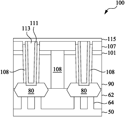
1. A method of forming a semiconductor device, the method comprising:
forming a gate structure over a first fin, wherein the first fin protrudes above a substrate, and the gate structure is surrounded by a first interlayer dielectric (ILD) layer;
forming a trench in the first ILD layer adjacent to the first fin;
filling the trench with a first dummy material;
forming a second ILD layer over the first ILD layer and the first dummy material;
forming a first opening in the first ILD layer and the second ILD layer, wherein the first opening exposes a sidewall of the first dummy material;
lining sidewalls of the first opening with a second dummy material;
after lining the sidewalls of the first opening, forming a conductive material in the first opening;
after forming the conductive material, removing the first dummy material from the trench and removing the second dummy material from the first opening; and
after the removing, sealing the first opening and the trench by forming a dielectric layer over the second ILD layer.
|