| CPC H01L 27/0924 (2013.01) [H01L 29/41791 (2013.01); H01L 29/66553 (2013.01); H01L 29/66795 (2013.01); H01L 29/7851 (2013.01)] | 20 Claims |
|
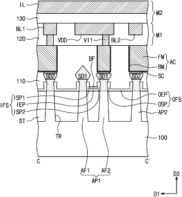
1. A semiconductor device, comprising:
a first active pattern on a substrate, wherein the first active pattern comprises a first active fin and a second active fin, which are adjacent to each other in a first direction;
a device isolation layer defining the first active pattern;
a gate electrode crossing the first active pattern;
a first source/drain pattern and a second source/drain pattern provided on the first active fin and the second active fin, respectively;
an inner fin spacer interposed between the first and second source/drain patterns; and
a buffer layer provided on the device isolation layer between the first and second active fins,
wherein the inner fin spacer comprises:
a first inner spacer portion contacting the first source/drain pattern;
a second inner spacer portion contacting the second source/drain pattern; and
an inner extended portion extending from the first and second inner spacer portions, wherein the inner extended portion is between the first and second active fins,
wherein the buffer layer has a dielectric constant higher than a dielectric constant of the inner fin spacer,
wherein a top surface of the buffer layer is at a level lower than a top surface of the inner fin spacer.
|