| CPC H01L 27/0886 (2013.01) [H01L 21/31111 (2013.01); H01L 21/32135 (2013.01); H01L 21/32139 (2013.01); H01L 21/823431 (2013.01); H01L 21/823437 (2013.01); H01L 21/823821 (2013.01); H01L 21/823878 (2013.01); H01L 27/0924 (2013.01); H01L 29/0649 (2013.01); H01L 29/42376 (2013.01); H01L 29/4966 (2013.01); H01L 29/4975 (2013.01); H01L 29/517 (2013.01); H01L 29/66545 (2013.01); H01L 21/823828 (2013.01)] | 20 Claims |
|
1. A device, comprising:
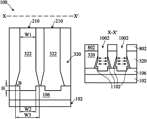
a first fin and a second fin extending from a substrate and extending in a first direction, the first fin having a first gate region and the second fin having a second gate region and a shallow trench isolation (STI) structure interposing the first and second fins;
a first metal gate structure disposed over the first gate region and a second metal gate structure disposed over the second gate region, wherein the first and second metal gate structures are separated by a cut gate region and wherein the first and second metal gate structures extend in a second direction, the second direction perpendicular to the first direction; and
a dielectric layer disposed in the cut gate region, wherein the dielectric layer extends below a top surface of the STI structure by a distance, wherein the dielectric layer in the cut gate region includes a first width within the STI structure, a second width measured adjacent the top surface of the STI structure, and a third width measured above the second width, wherein the second width is greater than the first and third width;
wherein the first metal gate structure has a first face abutting the cut gate region, wherein the first face is parallel the first direction and the first face has the second width measured in the first direction adjacent the top surface of the STI structure and the first metal gate structure has the third width above the second width and measured in the first direction.
|