| CPC H01L 25/0753 (2013.01) [H01L 33/54 (2013.01); H01L 33/62 (2013.01); H01L 2933/005 (2013.01); H01L 2933/0066 (2013.01)] | 9 Claims |
|
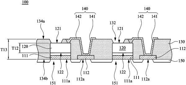
1. A light-emitting package, comprising:
an encapsulating member, having a first surface and a second surface opposite to the first surface;
a plurality of light-emitting components, respectively having a plurality of light-emitting surfaces and a plurality of back surfaces opposite to the light-emitting surfaces, wherein the light-emitting components are disposed in the encapsulating member, and the light-emitting surfaces are exposed on the first surface;
a plurality of first electrode pads, respectively having a plurality of first bonding surfaces and disposed in the encapsulating member, the light-emitting components respectively disposed on the first electrode pads and electrically connected to the first electrode pads, wherein the first bonding surfaces are exposed on the second surface and flush with the second surface;
a plurality of second electrode pads, respectively having a plurality of second bonding surfaces and disposed in the encapsulating member, wherein the second bonding surfaces are exposed on the second surface and flush with the second surface;
a plurality of conductive connection structures, passing through the encapsulating member and electrically connected to the light-emitting components and the second electrode pads, thereby causing that each of the light-emitting components is electrically connected to one of the first electrode pads and one of the second electrode pads; and
a protective layer, formed on the second surface and having a plurality of openings, wherein the openings expose the first bonding surfaces and the second bonding surfaces respectively,
wherein each of the first electrode pads does not extend to enter any one of the openings,
wherein each of the second electrode pads does not extend to enter any one of the openings.
|