| CPC H01L 25/0657 (2013.01) [H01L 21/568 (2013.01); H01L 23/3128 (2013.01); H01L 23/3135 (2013.01); H01L 23/5383 (2013.01); H01L 23/5386 (2013.01); H01L 24/16 (2013.01); H01L 24/81 (2013.01); H01L 25/50 (2013.01); H01L 2224/16145 (2013.01); H01L 2224/16227 (2013.01)] | 18 Claims |
|
1. A semiconductor device package, comprising:
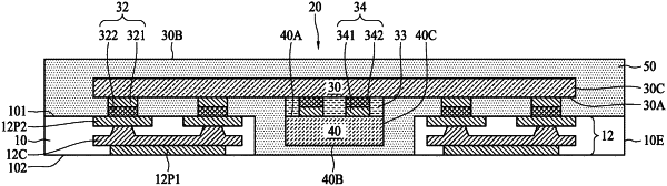
a substrate comprising a circuit layer, the substrate including a first surface and a second surface opposite to the first surface, at least one recess recessed from the second surface and partially exposing the circuit layer, and a bottom surface of the circuit layer in the recess is recessed from the second surface of the substrate;
a first electronic component disposed above the first surface;
a second electronic component stacked adjacent to the first electronic component;
an encapsulation layer at least encapsulating the second electronic component and partially covering the second surface of the substrate; and
an electrical conductor extending from the second surface of the substrate into the recess of the substrate, and contacting the bottom surface of the circuit layer,
wherein a space is defined between the encapsulation layer and the electrical conductor.
|