| CPC H01L 25/0657 (2013.01) [H01L 21/56 (2013.01); H01L 21/561 (2013.01); H01L 21/568 (2013.01); H01L 21/6835 (2013.01); H01L 21/76871 (2013.01); H01L 21/76877 (2013.01); H01L 23/3128 (2013.01); H01L 23/49816 (2013.01); H01L 23/49838 (2013.01); H01L 23/5389 (2013.01); H01L 24/05 (2013.01); H01L 24/06 (2013.01); H01L 24/14 (2013.01); H01L 24/19 (2013.01); H01L 24/20 (2013.01); H01L 25/105 (2013.01); H01L 25/50 (2013.01); H01L 21/563 (2013.01); H01L 23/3107 (2013.01); H01L 2221/68345 (2013.01); H01L 2221/68359 (2013.01); H01L 2221/68372 (2013.01); H01L 2224/0401 (2013.01); H01L 2224/04105 (2013.01); H01L 2224/05124 (2013.01); H01L 2224/12105 (2013.01); H01L 2224/214 (2013.01); H01L 2224/32145 (2013.01); H01L 2224/32225 (2013.01); H01L 2224/48091 (2013.01); H01L 2224/73265 (2013.01); H01L 2224/73267 (2013.01); H01L 2224/92244 (2013.01); H01L 2225/0651 (2013.01); H01L 2225/06506 (2013.01); H01L 2225/06568 (2013.01); H01L 2225/1035 (2013.01); H01L 2225/1058 (2013.01); H01L 2924/15311 (2013.01)] | 20 Claims |
|
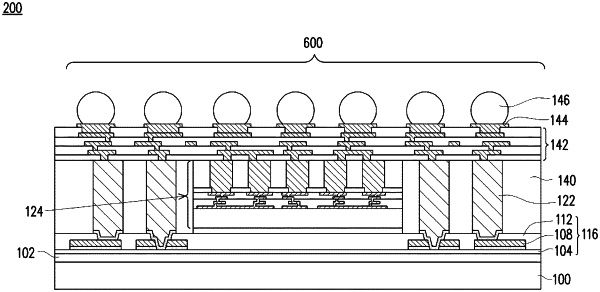
1. A method comprising:
forming a first redistribution structure comprising:
depositing a first dielectric layer over a carrier substrate;
forming a first conductive feature and a second conductive feature on the first dielectric layer, wherein the second conductive feature is provided with a gap that exposes the first dielectric layer; and
depositing a second dielectric layer on the first conductive feature and the second conductive feature;
forming a first opening and a second opening in the second dielectric layer, wherein the first opening exposes the first conductive feature and the second opening exposes the second conductive feature and the gap;
forming a first via on the first conductive feature and partially in the first opening;
forming a second via on the second conductive feature and partially in the second opening and the gap;
attaching a die to the first redistribution structure adjacent the first via and the second via; and
encapsulating the die, the first via, and the second via with an encapsulant.
|