| CPC H01L 25/0657 (2013.01) [H01L 23/3114 (2013.01); H01L 23/49822 (2013.01); H01L 23/49827 (2013.01)] | 20 Claims |
|
1. A semiconductor structure, comprising:
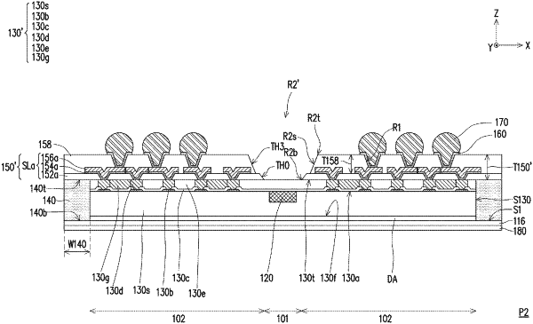
a semiconductor die, comprising a sensor device, a dielectric layer and a semiconductor substrate with a first region and a second region adjacent to the first region, the dielectric layer extending over the first region and the second region of the semiconductor substrate, and the sensor device being embedded in the semiconductor substrate within the first region, wherein the dielectric layer covers a first surface of the sensor device exposing from a second surface of the semiconductor substrate;
an insulating encapsulation, laterally encapsulating the semiconductor die and covering a sidewall of the semiconductor die;
a die attach film, disposed on a third surface of the semiconductor substrate, the third surface being opposite to the second surface, wherein a surface of the die attach film being opposite to the third surface is substantially coplanar to a fourth surface of the insulating encapsulation;
a passivation layer, located on the semiconductor die, wherein a recess penetrates through the passivation layer over the first region and is overlapped with the sensor device, and through holes penetrate through the passivation layer over the second region, wherein the recess has a side surface and a bottom surface connecting to the side surface, and the entire side surface and the entire bottom surface are dielectric surfaces, wherein a portion of the dielectric layer covering the sensor device within the first region is exposed by the recess;
solder balls, located on the passivation layer over the second region, and electrically connected to the semiconductor die, wherein the passivation layer is between the insulating encapsulation and the solder balls, and each of the solder balls is located at a respective one of the through holes, respectively; and
a protection layer, located on the semiconductor die, wherein the semiconductor die and the insulating encapsulation are between the passivation layer and the protection layer.
|