| CPC H01L 24/81 (2013.01) [H01L 24/13 (2013.01); H01L 24/16 (2013.01); H01L 25/0657 (2013.01); H01L 25/50 (2013.01); H01L 2224/131 (2013.01); H01L 2224/1308 (2013.01); H01L 2224/13017 (2013.01); H01L 2224/13076 (2013.01); H01L 2224/13082 (2013.01); H01L 2224/13144 (2013.01); H01L 2224/16058 (2013.01); H01L 2224/16148 (2013.01); H01L 2224/16225 (2013.01); H01L 2224/16238 (2013.01); H01L 2224/73204 (2013.01); H01L 2224/81143 (2013.01); H01L 2224/81191 (2013.01); H01L 2224/81815 (2013.01); H01L 2225/06513 (2013.01); H01L 2225/06593 (2013.01); H01L 2924/01322 (2013.01); H01L 2924/381 (2013.01)] | 20 Claims |
|
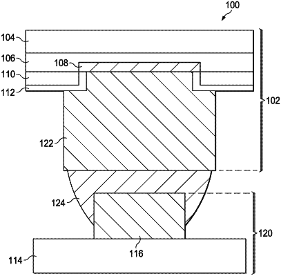
1. A semiconductor package comprising:
a first substrate having a conductive land;
a conductive bump attached to the conductive land and extending away from the conductive land, wherein an end surface of the conductive bump distal from the conductive land has a first width;
a second substrate;
a conductive trace on a first side of the second substrate facing the first substrate, wherein a first surface of the conductive trace distal from the second substrate has a second width smaller than the first width, wherein a first sidewall of the conductive trace has a first height, wherein the end surface of the conductive bump is spaced apart from the first surface of the conducive trace by a first distance smaller than the first height; and
a conductive material bonding the conductive bump to the conductive trace, wherein the conductive material extends along and covers the first sidewall of the conductive trace by at least half the first height.
|