| CPC H01L 23/585 (2013.01) [H01L 21/4857 (2013.01); H01L 21/568 (2013.01); H01L 21/6835 (2013.01); H01L 23/3128 (2013.01); H01L 23/485 (2013.01); H01L 24/19 (2013.01); H01L 24/20 (2013.01); H01L 21/561 (2013.01); H01L 25/105 (2013.01); H01L 25/50 (2013.01); H01L 2221/68345 (2013.01); H01L 2221/68372 (2013.01); H01L 2221/68381 (2013.01); H01L 2224/04105 (2013.01); H01L 2224/12105 (2013.01); H01L 2224/16227 (2013.01); H01L 2224/32225 (2013.01); H01L 2224/73267 (2013.01); H01L 2224/92244 (2013.01); H01L 2225/1035 (2013.01); H01L 2225/1041 (2013.01); H01L 2225/1058 (2013.01); H01L 2225/1082 (2013.01); H01L 2924/1434 (2013.01); H01L 2924/1436 (2013.01); H01L 2924/15311 (2013.01)] | 20 Claims |
|
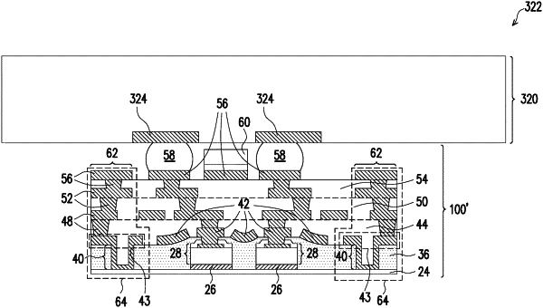
1. A method comprising:
placing a plurality of conductive pins over a carrier;
placing a device die over the carrier;
encapsulating the plurality of conductive pins and the device die in an encapsulant, wherein a top layer of the encapsulant covers the device die and the plurality of conductive pins;
forming openings in the top layer of the encapsulant to reveal the plurality of conductive pins and conductive features of the device die; and
forming a first plurality of redistribution lines extending into the openings to contact the conductive features of the device die, wherein the device die, the plurality of conductive pins, and the first plurality of redistribution lines form parts of a package.
|