| CPC H01L 23/5389 (2013.01) [H01L 21/486 (2013.01); H01L 21/4853 (2013.01); H01L 21/4857 (2013.01); H01L 21/4875 (2013.01); H01L 21/4889 (2013.01); H01L 21/561 (2013.01); H01L 21/565 (2013.01); H01L 21/6835 (2013.01); H01L 23/3114 (2013.01); H01L 23/3135 (2013.01); H01L 23/3675 (2013.01); H01L 23/49833 (2013.01); H01L 23/49838 (2013.01); H01L 23/5383 (2013.01); H01L 23/5384 (2013.01); H01L 23/5386 (2013.01); H01L 23/66 (2013.01); H01L 24/19 (2013.01); H01L 24/20 (2013.01); H01Q 1/2283 (2013.01); H01L 23/3128 (2013.01); H01L 23/49822 (2013.01); H01L 23/49827 (2013.01); H01L 24/29 (2013.01); H01L 24/32 (2013.01); H01L 24/73 (2013.01); H01L 24/92 (2013.01); H01L 2221/68345 (2013.01); H01L 2221/68359 (2013.01); H01L 2223/6677 (2013.01); H01L 2224/04105 (2013.01); H01L 2224/12105 (2013.01); H01L 2224/19 (2013.01); H01L 2224/214 (2013.01); H01L 2224/2919 (2013.01); H01L 2224/32225 (2013.01); H01L 2224/73267 (2013.01); H01L 2224/92244 (2013.01); H01L 2924/141 (2013.01); H01L 2924/143 (2013.01); H01L 2924/1421 (2013.01); H01L 2924/1431 (2013.01); H01L 2924/1434 (2013.01); H01Q 1/243 (2013.01)] | 20 Claims |
|
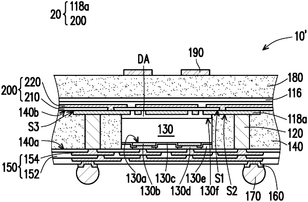
1. A package structure, comprising:
a metal layer, having a first surface and a second surface opposite to the first surface;
a semiconductor die, located on the second surface of the metal layer;
an encapsulant, laterally encapsulating the semiconductor die;
antenna elements, located over the first surface of the metal layer; and
conductive pillars, disposed on and electrically connected to the semiconductor die, wherein the conductive pillars are spaced apart from the metal layer.
|
|
10. A package structure, comprising:
a semiconductor die, molded in an encapsulant and having an active surface and a backside surface opposite to the active surface;
a metal layer, located on the backside surface of the semiconductor die, wherein the metal layer has a first surface and a second surface opposite to the first surface, the second surface of the metal layer is covered by the encapsulant and disposed with the semiconductor die, and the first surface of the metal layer is free from the encapsulant, wherein the first surface of the metal layer is coplanar with a third surface of the encapsulant;
a first redistribution circuit structure, located on and electrically connected to the semiconductor die, the semiconductor die being located between the metal layer and the first redistribution circuit structure;
conductive terminals, located on and electrically connected to the first redistribution circuit structure, wherein the first redistribution circuit structure is located between the conductive terminals and the semiconductor die; and
antenna elements, located over the first surface of the metal layer, wherein the metal layer is located between the semiconductor die and the antenna elements, and the antenna elements are electrically connected to the metal layer in a manner of electrical coupling.
|
|
18. A manufacturing method of a package structure, comprising:
forming a metal layer having a first surface and a second surface opposite to the first surface;
disposing a semiconductor die over the second surface of the metal layer;
molding the semiconductor die in an encapsulant, the second surface of the metal layer being covered by the encapsulant, the first surface of the metal layer being free from the encapsulant, and the first surface of the metal layer being coplanar with a third surface of the encapsulant;
forming a first redistribution circuit structure over the semiconductor die and a fourth surface of the encapsulant, the fourth surface being opposite to the third surface, and the semiconductor die being located between the metal layer and the first redistribution circuit structure;
disposing conductive terminals on the first redistribution circuit structure, the first redistribution circuit structure being located between and electrically connected to the conductive terminals and the semiconductor die; and
forming antenna elements over the semiconductor die and the third surface of the encapsulant, the metal layer being located between the semiconductor die and the antenna elements, and the antenna elements being electrically connected to the metal layer in a manner of electrical coupling.
|