| CPC H01L 23/5384 (2013.01) [H01L 21/56 (2013.01); H01L 21/76802 (2013.01); H01L 23/31 (2013.01); H01L 23/367 (2013.01); H01L 23/4006 (2013.01); H01L 23/4012 (2013.01); H01L 23/5385 (2013.01); H01L 24/14 (2013.01); H01L 25/0657 (2013.01)] | 20 Claims |
|
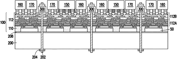
1. A semiconductor device, comprising:
a first die, the first die comprising a chamfered corner and a seal ring, the seal ring of the first die being along the chamfered corner;
an encapsulant over a front-side surface of the first die, the encapsulant at least partially surrounding the first die;
a redistribution structure on the encapsulant;
a thermal interface material on a back-side surface of the first die, the back-side surface being opposite the front-side surface;
a thermal module thermally and physically coupled to the back-side surface of the first die with the thermal interface material; and
a bolt extending through the redistribution structure and the thermal module, the bolt being adjacent to the chamfered corner.
|