| CPC H01L 23/5226 (2013.01) [H01L 21/7682 (2013.01); H01L 21/76802 (2013.01); H01L 21/76831 (2013.01); H01L 21/76843 (2013.01); H01L 21/76877 (2013.01); H01L 23/53295 (2013.01)] | 20 Claims |
|
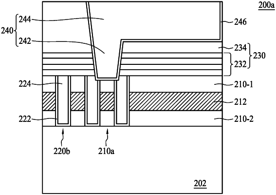
1. A semiconductor structure comprising:
a substrate;
a plurality of conductive features disposed over the substrate, wherein each of the conductive features comprises:
a first metal layer;
a second metal layer between the first metal layer and the substrates;
a 2D material layer disposed between the first metal layer and the second metal layer:
an isolation structure between the conductive features and separating the conductive features from each other; and
a conductive via disposed over one of the conductive features, wherein a bottom of the conductive via is coupled to the first metal layer.
|