| CPC H01L 23/49816 (2013.01) [H01L 21/486 (2013.01); H01L 21/4857 (2013.01); H01L 21/565 (2013.01); H01L 23/3135 (2013.01); H01L 23/49822 (2013.01); H01L 23/49833 (2013.01); H01L 23/49838 (2013.01); H01L 23/5385 (2013.01); H01L 23/5386 (2013.01); H01L 24/13 (2013.01); H01L 24/16 (2013.01); H01L 24/73 (2013.01); H01L 25/0655 (2013.01); H01L 2224/13147 (2013.01); H01L 2224/13582 (2013.01); H01L 2224/16227 (2013.01); H01L 2224/16235 (2013.01); H01L 2224/73204 (2013.01); H01L 2924/1434 (2013.01); H01L 2924/14335 (2013.01); H01L 2924/35 (2013.01)] | 8 Claims |
|
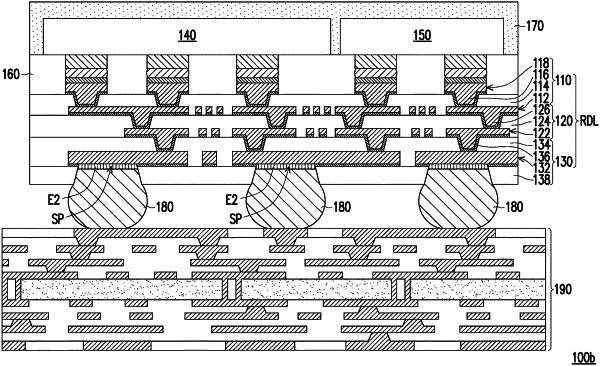
1. A package structure, comprising:
a redistribution layer, comprising a plurality of redistribution circuits, a plurality of photoimageable dielectric layers, a plurality of conductive through holes, and a plurality of chip pads, wherein the redistribution circuits and the photoimageable dielectric layers are disposed in an alternating manner, and the conductive through holes penetrate through the photoimageable dielectric layers and are electrically connected to the redistribution circuits, wherein one of the photoimageable dielectric layers located on opposite two outermost sides has an upper surface, the chip pads are located on the upper surface and are electrically connected to the redistribution circuits through the conductive through holes, the other one of the photoimageable dielectric layers located on the opposite two outermost sides has a plurality of openings, the openings expose portions of the redistribution circuits to define a plurality of solder ball pads, and line widths and line spacings of the redistribution circuits decrease in a direction from the solder ball pads towards the chip pads;
a chip assembly, disposed on the chip pads, electrically connected to the chip pads, wherein the chip assembly comprises at least two chips with different sizes;
a plurality of solder balls, disposed on the solder ball pads, electrically connected to the solder ball pads; and
a molding compound, at least covering the chip assembly, wherein the redistribution layer comprises a first redistribution layer, a second redistribution layer, and a third redistribution layer, the redistribution circuits comprises a first redistribution circuit, a second redistribution circuit, and a third redistribution circuit, the photoimageable dielectric layers comprise a first photoimageable dielectric layer, a second photoimageable dielectric layer, a third photoimageable dielectric layer, and a fourth photoimageable dielectric layer, and the conductive through holes comprise a plurality of first conductive through holes, a plurality of second conductive through holes, and a plurality of third conductive through holes,
wherein the first redistribution layer comprises the chip pads, the first redistribution circuit, the first photoimageable dielectric layer, and the first conductive through holes penetrating through the first photoimageable dielectric layer, the first photoimageable dielectric layer has the upper surface, and the chip pads are electrically connected to the first redistribution circuit through the first conductive through holes,
wherein the second redistribution layer comprises the second redistribution circuit, the second photoimageable dielectric layer, and the second conductive through holes penetrating through the second photoimageable dielectric layer, and the second conductive through holes are electrically connected to the first redistribution circuit and the second redistribution circuit,
wherein the third redistribution layer comprises the third redistribution circuit, the third photoimageable dielectric layer, the fourth photoimageable dielectric layer, and the third conductive through holes penetrating through the third photoimageable dielectric layer, the third conductive through holes are electrically connected to the second redistribution circuit and the third redistribution circuit, the fourth photoimageable dielectric layer covers the third photoimageable dielectric layer and the third redistribution circuit and has the openings, and the openings expose portions of the third redistribution circuit to define the solder ball pads,
wherein a line width and a line spacing of the third redistribution circuit are greater than a line width and a line spacing of the second redistribution circuit, and the line width and the line spacing of the second redistribution circuit are greater than a line width and a line spacing of the first redistribution circuit,
wherein a depth of each of the second conductive through holes is equal to a depth of each of the third conductive through holes, and a depth of each of the first conductive through holes is less than the depth of each of the second conductive through holes.
|