| CPC H01L 22/32 (2013.01) [H01L 22/20 (2013.01); H01L 23/544 (2013.01); H01L 24/03 (2013.01); H01L 24/08 (2013.01)] | 20 Claims |
|
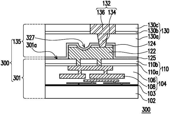
1. A semiconductor structure, comprising:
an interconnect structure, disposed over a substrate;
a pad structure, disposed over and electrically connected to the interconnect structure, wherein the pad structure comprises a metal pad and a dielectric cap on the metal pad, and the pad structure has a probe mark recessed from a top surface of the dielectric cap into a top surface of the metal pad;
a protective layer, conformally covering the top surface of the dielectric cap and the probe mark; and
a bonding structure, disposed over the protective layer, wherein the bonding structure comprises:
a bonding dielectric layer at least comprising a first bonding dielectric material and a second bonding dielectric material on the first bonding dielectric material; and
a first bonding metal layer disposed in the bonding dielectric layer and penetrating through the protective layer and the dielectric cap to contact the metal pad.
|