| CPC H01L 21/823821 (2013.01) [H01L 21/823814 (2013.01); H01L 21/823828 (2013.01); H01L 27/0924 (2013.01); H01L 29/4966 (2013.01); H01L 29/66545 (2013.01); H01L 29/66795 (2013.01); H01L 29/785 (2013.01); H01L 21/823842 (2013.01); H01L 29/513 (2013.01); H01L 29/517 (2013.01)] | 20 Claims |
|
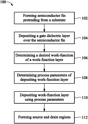
1. A semiconductor device comprising:
an n-type transistor comprising:
a first fin extending from a substrate;
a first gate dielectric layer over the first fin; and
a first work-function layer over the first gate dielectric layer, wherein the first work-function layer directly contacts the first gate dielectric layer; and
a p-type transistor comprising:
a second fin extending from the substrate;
a second gate dielectric layer over the second fin; and
a second work-function layer over the second gate dielectric layer, wherein the second work-function layer directly contacts the second gate dielectric layer, wherein the first work-function layer and the second work-function layer comprise a first work-function material, and wherein the first work-function layer has a first proportion of a first crystalline orientation and the second work-function layer has a second proportion of the first crystalline orientation different than the first proportion of the first crystalline orientation.
|