| CPC H01L 21/76898 (2013.01) [H01L 21/76831 (2013.01); H01L 21/76877 (2013.01); H01L 23/481 (2013.01); H01L 2224/13 (2013.01)] | 20 Claims |

|
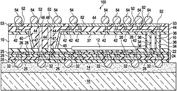
1. A method comprising:
forming a first through-via extending from a first side of a semiconductor substrate into the semiconductor substrate, wherein the semiconductor substrate comprises a first surface on the first side;
polishing the semiconductor substrate so that a second surface of the semiconductor substrate is formed, with the second surface being opposite to the first surface, wherein the semiconductor substrate comprises a semiconductor material continuously extends from the first surface to the second surface, and wherein after the polishing, the first through-via is revealed through the second surface;
etching the semiconductor substrate from a second side of the semiconductor substrate to form a first through-opening, wherein the first side and the second side are opposite sides of the semiconductor substrate;
filling the first through-opening with a dielectric material to form a dielectric region; and
forming a second through-via penetrating through the dielectric region.
|