| CPC H01L 21/385 (2013.01) [G02F 1/1368 (2013.01); G02F 1/13439 (2013.01); G02F 1/134309 (2013.01); H01L 27/124 (2013.01); H01L 27/1225 (2013.01); H01L 29/41733 (2013.01); H01L 29/4908 (2013.01); H01L 29/4958 (2013.01); H01L 29/4966 (2013.01); H01L 29/513 (2013.01); H01L 29/518 (2013.01); H01L 29/66969 (2013.01); H01L 29/7869 (2013.01); H01L 29/78696 (2013.01); G02F 2201/123 (2013.01)] | 9 Claims |

|
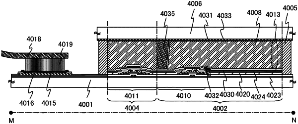
1. A liquid crystal display device comprising:
a gate electrode;
a gate insulating layer over the gate electrode;
an oxide semiconductor layer over the gate insulating layer, the oxide semiconductor layer comprising indium, gallium, and zinc;
a source electrode and a drain electrode over the oxide semiconductor layer, each of the source electrode and the drain electrode comprising a metal film comprising copper;
a silicon oxide layer over the oxide semiconductor layer, the source electrode, and the drain electrode;
a silicon nitride layer over the silicon oxide layer;
a pixel electrode over the silicon nitride layer, the pixel electrode comprising indium tin oxide; and
a liquid crystal layer over the pixel electrode,
wherein the metal film of the source electrode or the drain electrode comprises a first region where a metal oxide region comprising copper is provided over a top surface of the metal film and a second region where the metal oxide region is not provided over the top surface of the metal film,
wherein the pixel electrode is in contact with the second region through an opening provided in the silicon oxide layer and the silicon nitride layer,
wherein the second region is overlapped with the opening,
wherein the first region is not overlapped with the opening, and
wherein a thickness of the second region is smaller than a thickness of the first region.
|