| CPC H01C 7/1006 (2013.01) [H01C 7/102 (2013.01); H01C 7/108 (2013.01)] | 11 Claims |
|
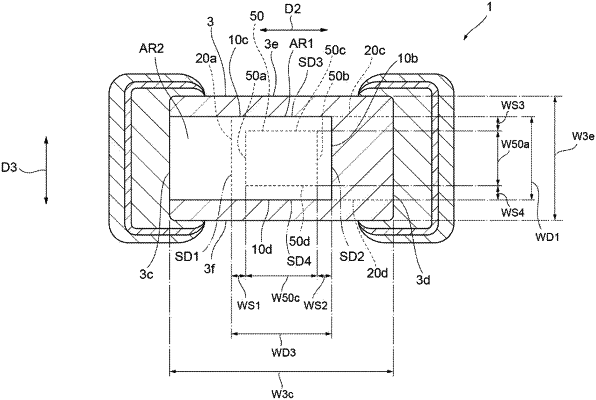
1. A chip varistor comprising:
an element body;
first and second internal electrodes (i) in the element body, (ii) that oppose each other in a first direction, (iii) spaced from each other in the first direction, and (iv) that are connected to different external electrodes; and
at least one intermediate conductor (i) in the element body between the first and second internal electrodes, (ii) that opposes the first and second internal electrodes in the first direction and (iii) spaced from the first and second internal electrodes in the first direction, wherein:
the first and second internal electrodes overlap in the first direction to define an overlapping region having a first outer edge when viewed in the first direction;
the at least one intermediate conductor includes a second outer edge when viewed in the first direction; and
the second outer edge is spaced inwardly from the first outer edge in the overlapping region when viewed in the first direction.
|