| CPC G11C 29/787 (2013.01) [G11C 7/1039 (2013.01); G11C 15/04 (2013.01); G11C 16/3445 (2013.01); G11C 16/3459 (2013.01); G11C 29/4401 (2013.01); G11C 29/76 (2013.01)] | 20 Claims |
|
1. A memory device, comprising:
a memory cell array comprising a plurality of regular memory blocks and a plurality of redundant memory blocks, wherein the plurality of regular memory blocks are configured to store data;
a redundant fuse circuit comprising a plurality of fuse groups configured to record a plurality of repair information, wherein each of the plurality of repair information is associated with a corresponding one of the plurality of redundant memory blocks, and each of the plurality of repair information comprises:
a repair address configured to indicate a position of the regular memory block that is to be replaced by the associated redundant memory block;
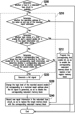
a first enable bit configured to record a usage state of a corresponding one of the plurality of fuse groups, wherein a first logic state of the first enable bit indicates that the corresponding one of the plurality of fuse groups has been used, and a second logic state of the first enable bit indicates that the corresponding one of the plurality of fuse groups has not been used and is an available fuse group; and
a second enable bit configured to enable a corresponding one of the plurality of redundant memory blocks, wherein a first logic state of the second enable bit indicates that the corresponding one of the plurality of redundant memory blocks is bad, and a second logic state of the second enable bit indicates that the corresponding one of the plurality of redundant memory blocks is not bad; and
a memory controller coupled with the memory cell array and the redundant fuse circuit and configured to perform an operation on a target memory block according to an operation address and to determine whether the target memory block is bad, wherein the memory controller comprises a plurality of determining circuits, and each of the plurality of determining circuits generates a hit signal according to the operation address, the repair address, the first enable bit, and the second enable bit,
wherein when the target memory block is bad, and the determining circuit of the memory controller generates the hit signal, the memory controller disables the redundant memory block that is bad according to the hit signal.
|