| CPC G11C 17/165 (2013.01) [G11C 7/1069 (2013.01); G11C 7/1096 (2013.01); G11C 17/04 (2013.01); G11C 17/18 (2013.01)] | 12 Claims |
|
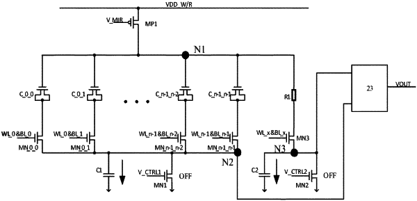
1. A read-write circuit of one-time programmable memory, comprising:
an antifuse array, comprising:
n*n antifuse units, wherein each of the n*n antifuse units comprises an antifuse element and a switching element coupled together, wherein a first end of one of the n*n antifuse units is coupled to a first node, and a second end of said antifuse unit is connected to a second node, wherein a control end of the switching element in each of the n*n antifuse units is respectively coupled to an AND signal of a word line signal and a bit line signal different from word line signal, wherein a first node is coupled to a mirror current source, wherein the mirror current source is electrically connected to a first voltage source;
a first capacitor and a first switching device connected in parallel between the second node and a second voltage source, wherein a control terminal of the first switching device is connected to a first control signal;
a reference array, comprising:
a reference resistor and a reference switch element connected in series between the first node and the third node, wherein a control end of the reference switch element is coupled to an OR signal of n*n AND signals;
a second capacitor and a second switching device connected in parallel between the third node and the second voltage source, wherein a control terminal of the second switching device is coupled to a second control signal; and
a comparison circuit, wherein a first input terminal of the comparison circuit is coupled to the second node, a second input terminal is coupled to the third node, and wherein the comparison circuit compares a voltage at the second node and a voltage at the third node and determines if a programed operation occurs at said antifuse unit.
|