| CPC G11C 5/147 (2013.01) [G11C 7/1084 (2013.01); G11C 17/165 (2013.01); G11C 17/18 (2013.01)] | 6 Claims |
|
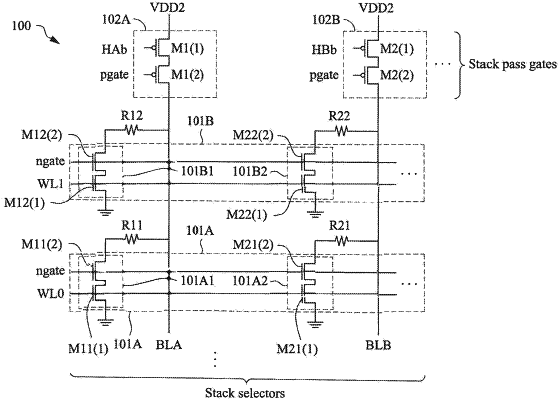
1. A memory array comprising:
a plurality of N-stack pass gates, each N-stack pass gate comprising a stage-1 PMOS core device and a stage-N PMOS core device in series with the stage-1 PMOS core device, each stage-1 PMOS coupled to a voltage supply;
a plurality of enable lines, each enable line driving a corresponding stage-1 PMOS core device;
a plurality of N-stack selectors, each N-stack selector comprising a plurality of NMOS stacks, each NMOS stack comprising:
a stage-1 NMOS core device each stage-1 NMOS core device coupled to a ground rail; and
a stage-N NMOS core device in series with the stage-1 NMOS core;
a plurality of word lines, each word line driving the plurality of stage-1 NMOS core devices of a corresponding N-stack selector; and
a matrix of resistive elements, each resistive element coupled between a stage-N PMOS device of a corresponding N-stack pass gate and a stage-N NMOS device of a corresponding NMOS stack of a corresponding N-stack selector;
wherein each voltage supply is greater than a breakdown voltage for each of the stage-1 PMOS core device, the stage-N PMOS core device, the stage-1 NMOS core device, and the stage-N NMOS core device.
|