| CPC G09G 3/3233 (2013.01) [G09G 2300/0426 (2013.01); G09G 2300/0819 (2013.01); G09G 2300/0842 (2013.01); G09G 2320/0257 (2013.01)] | 20 Claims |
|
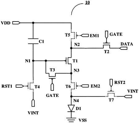
1. A pixel circuit, comprising: a driving circuit, a data writing circuit, a first reset circuit, a first light emission control circuit and a light emitter element, wherein
the driving circuit comprises a control terminal, a first terminal and a second terminal, and the driving circuit is configured to control a driving current, which passes through the first terminal and the second terminal, for driving the light emitter element to emit light;
the first light emission control circuit is configured to apply a first voltage to the first terminal of the driving circuit in response to a first light emission control signal in an initialization stage;
the first reset circuit is configured to apply a reset voltage to the control terminal of the driving circuit in response to a first reset signal;
the pixel circuit further comprises a second light emission control circuit, the second light emission control circuit is configured to apply the driving current to the light emitter element in response to a second light emission control signal, wherein
the second light emission control signal is different from the first light emission control signal;
the pixel circuit further comprises a compensation circuit, the compensation circuit is electrically connected with the control terminal of the driving circuit, the first terminal of the driving circuit, and the first reset circuit, and the compensation circuit is configured to store the data signal that is written in and compensate the driving circuit in response to the scan signal;
in the initialization stage, the first reset signal and the first light emission control signal are simultaneously turn-on signals, and the second light emission control signal is a turn-off signal, and the first light emission control circuit applies the first voltage to the first terminal of the driving circuit in response to the first light emission control signal, and the first reset circuit is configured to apply the reset voltage to the control terminal of the driving circuit in response to the first reset signal, so that the control terminal of the driving circuit and the first terminal of the driving circuit are in a fixed bias state; and
in a data writing and compensation stage after the initialization stage, the driving circuit and the compensation circuit are turned on, the data writing circuit writes the data signal to the control terminal of the driving circuit successively via the driving circuit and the compensation circuit in response to the scan signal, and the compensation circuit stores the data signal that is written in.
|