| CPC G09G 3/3225 (2013.01) [G09G 3/3266 (2013.01); G09G 3/3275 (2013.01); G09G 2300/0819 (2013.01); G09G 2300/0842 (2013.01); G09G 2310/08 (2013.01); G09G 2320/0626 (2013.01)] | 17 Claims |
|
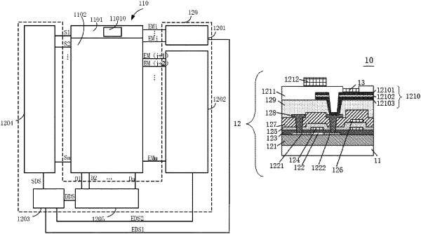
1. A display panel comprising:
a display region, the display region comprising a first display region and a second display region, the first display region comprising a transparent sub-display region, the transparent sub-display region having a light transmittance higher than a light transmittance of the second display region;
a first light emission controller and a second light emission controller, the first light emission controller being configured to provide a light emission control signal to a plurality of pixel rows of the first display region, the second light emission controller being configured to provide a light emission control signal to a plurality of pixel rows of the second display region; and
a base substrate, a backplane module, and a light emitting layer that are stacked in sequence;
wherein the light emitting layer comprises a pixel anode, and the first light emission controller and the second light emission controller are configured to provide a light emission driving signal to the backplane module so that the backplane module drives the light emitting layer to emit light,
wherein the backplane module comprises a buffer layer, an active layer, a first gate insulating layer, a first gate layer, a second gate insulating layer, a second gate layer, an interlayer dielectric layer, a source/drain electrode layer, a planarization layer, an anode, a pixel defining layer and a support layer that are stacked in sequence.
|