| CPC G06F 30/398 (2020.01) [G06F 30/367 (2020.01); G06F 30/392 (2020.01); G06F 30/3953 (2020.01); G06F 30/373 (2020.01); G06F 2119/06 (2020.01)] | 20 Claims |
|
1. A method, comprising:
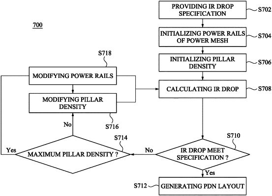
generating, based on design information for an integrated circuit, a circuit design that includes an initial power delivery network (PDN) for the integrated circuit;
performing a pre-layout simulation to the circuit design that includes the initial power delivery network, to determine whether the circuit design meets a predetermined specification;
generating a circuit layout of the integrated circuit when the circuit design meets the predetermined specification; and
adding at least one additional conductive pillar or at least one additional power rail in the initial power delivery network according to a relationship of a pillar density of the initial power delivery network and a maximum pillar density when the circuit design does not meet the predetermined specification.
|