| CPC G06F 3/0655 (2013.01) [G06F 3/0619 (2013.01); G06F 3/0673 (2013.01); G06F 11/1048 (2013.01); G11C 29/52 (2013.01)] | 16 Claims |
|
1. A memory device, comprising:
a memory chip including memory cells; and
a logic chip configured to control the memory chip,
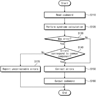
wherein the logic chip reads a codeword including N data units from the memory chip, and perform error correction decoding on the codeword to correct errors in M data units of the N data units, such that when the M data units correspond to a common hardware component specific to a sub-word line which connects memory cells of the memory chip, the logic chip is configured to correct the errors of the M data units by flipping bits of the errors of the M data units, and when the M data units do not correspond to the common hardware component of the memory chip, the logic chip is configured to process the errors of the M data units as an uncorrectable error,
N is a positive integer, and
M is a positive integer less than N,
wherein the logic chip includes:
a first error correction device configured to perform a first error correction encoding on a portion of the codeword to generate a first sub-codeword; and
a second error correction device configured to perform a second error correction encoding on a remaining portion of the codeword to generate a second sub-codeword.
|