| CPC G01R 31/2628 (2013.01) [G01K 7/01 (2013.01); G01R 31/2632 (2013.01)] | 8 Claims |
|
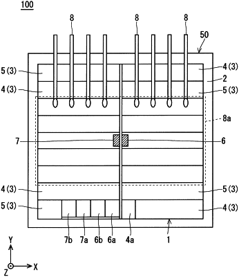
1. A semiconductor device, comprising
a semiconductor chip having a cell region made up of a plurality of cells which include cells corresponding to a transistor part and a diode part, respectively;
a first temperature detection part detecting a temperature of the transistor part; and
a second temperature detection part detecting a temperature of the diode part, wherein
the first temperature detection part is disposed in a cell corresponding to the transistor part,
the second temperature detection part is disposed in a cell corresponding to the diode part, and
the first temperature detection part detects the temperature of the transistor part independent of the second temperature detection part that detects the temperature of the diode part.
|