| CPC G01R 31/2621 (2013.01) [G01R 31/27 (2013.01); H03K 3/017 (2013.01); H03K 17/6871 (2013.01); H03K 2217/0063 (2013.01); H03K 2217/0072 (2013.01)] | 20 Claims |
|
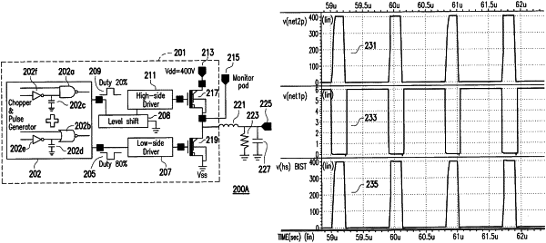
1. A reliability testing apparatus for stacked test gallium nitride field effect transistors (GaN FET) comprising:
a high side GaN FET test structure;
a low side GaN FET test structure;
a high side driver coupled to a gate of the high side GaN FET test structure;
a low side driver coupled to a gate of the low side GaN FET test structure;
an integrated driver circuit coupled to the high side and low side drivers and configured to generate drive signals capable of driving the high and low side GaN FET test structures,
wherein the high and low side GaN FET test structures are connected to a plurality of monitoring pads and
wherein the high and low side GaN FET test structures, the high and low side drivers, and the integrated driver circuit are all fabricated on a same semiconductor device layer during a front-end-of-line (FEOL) process.
|