| CPC G01N 21/3581 (2013.01) [G01N 21/3563 (2013.01); H01Q 1/525 (2013.01); H01Q 19/108 (2013.01); H01Q 21/062 (2013.01); H01Q 23/00 (2013.01); G01N 2021/3568 (2013.01); G01N 2201/061 (2013.01)] | 17 Claims |
|
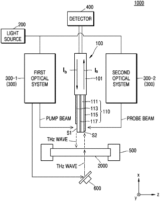
1. A hybrid probe, comprising:
a probe body including a wiring and extending in a first direction; and
a probe tip coupled to the probe body, the probe tip including:
a semiconductor substrate having a flat shape,
a first antenna on a first surface of the semiconductor substrate,
a second antenna on a second surface of the semiconductor substrate, the second surface being opposite the first surface, and
an isolation layer between the first and second surfaces of the semiconductor substrate,
wherein the hybrid probe operates in a reflection mode using the first antenna and the second antenna, and operates in a transmission mode using the second antenna.
|