US 11,680,340 B2
Low etch pit density 6 inch semi-insulating gallium arsenide wafers
Rajaram Shetty, Niskayuna, NY (US); Weiguo Liu, San Leandro, CA (US); and Morris Young, Fremont, CA (US)
Assigned to AXT, Inc., Fremont, CA (US)
Filed by AXT, Inc., Fremont, CA (US)
Filed on Dec. 11, 2019, as Appl. No. 16/711,019.
Claims priority of provisional application 62/779,039, filed on Dec. 13, 2018.
Prior Publication US 2020/0190696 A1, Jun. 18, 2020
Int. Cl. C30B 29/42 (2006.01); C30B 11/00 (2006.01); H01L 29/36 (2006.01); H01L 29/20 (2006.01); H01L 29/32 (2006.01); H01L 29/30 (2006.01); H01S 5/30 (2006.01)
CPC C30B 29/42 (2013.01) [C30B 11/002 (2013.01); C30B 11/006 (2013.01); H01L 29/20 (2013.01); H01L 29/32 (2013.01); H01L 29/36 (2013.01); H01L 29/30 (2013.01); H01S 5/3013 (2013.01)] 14 Claims
OG exemplary drawing
 
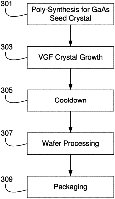
1. A semi-insulating gallium arsenide single crystal wafer having a diameter of 6 inches or greater without intentional dopants other than carbon for reducing dislocation density, an etch pit density of less than 1000 cm−2, and a resistivity of 1×10⁷ Ω-cm or more.